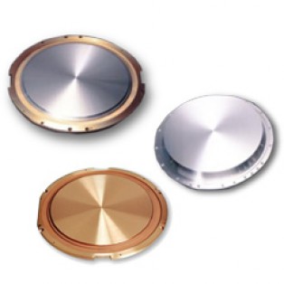
- Sputtering targets made using optimum manufacturing methods!
ULVAC has developed 2 types of tungsten targets for different manufacturing methods depending on the particular application required by the semiconductor process. One type was developed for products at a purity grade of 5N is an inexpensive and employs the powder sintering method. High-purity CVD tungsten target boasting a purity grade of 7N and using CVD (chemical vapor deposition) on sections requiring higher quality. - Low-particle targets
ULVAC has developed sputtering targets that suppress generation of particles that can be the source of problems in the sputtering process.
Gaseous elements are one factor in causing particle emissions especially in aluminum targets and we are working to lower emissions by utilizing a vacuum melting method in the refining and ingot purification processes. - Attaining high uniformity by adjusting the metal microstructure
ULVAC uses manufacturing processes that ensure high uniformity and a fine metal microstructure in most of its targets for semiconductor products including high purity cobalt targets and titanium targets.
Utilizing a fine metal microstructure having a high degree of uniformity for example allows uniform the magnetic flux leakage on the target surface of high purity cobalt targets. - Meticulous quality control system
Integrated process manufacturing at ULVAC takes product characteristics and contours into account during production. Sophisticated analysis/evaluation system such as the GD-MS (glow discharge mass spectrometer) ensure purity along with a high level of quality.
GDMS Analysis/Comparison for Various Tungsten Targets
| Target | Sinter-W | CVD-W |
|---|---|---|
| Na | ≤ 0.1 | ≤ 0.01 |
| K | ≤ 0.1 | ≤ 0.01 |
| Mg | – | ≤ 0.01 |
| Ca | – | ≤ 0.01 |
| Al | ≤ 1 | ≤ 0.03 |
| Cr | ≤ 1 | ≤ 0.03 |
| Fe | ≤ 1 | ≤ 0.03 |
| Ni | ≤ 1 | ≤ 0.03 |
| Cu | ≤ 1 | ≤ 0.01 |
| Th | ≤ 0.0005 | ≤ 0.0002 |
| U | ≤ 0.0005 | ≤ 0.0002 |
| O | ≤ 100 | ≤ 30 |
| C | ≤ 50 | ≤ 30 |
(ppm)
Sputtering Targets for Semiconductors
| Application Field | Materials | Manufacturing Method | Purpose of Use |
|---|---|---|---|
| Electrode materials | W (5N) | Powder sintering | Gate area |
| W (6N, 7N) | CVD | Gate etc. | |
| Co(5N) | Melting method | Gate area | |
| Ni(5N) | Melting method | Gate area | |
| Ti(5N) | Melting method | Lynear, Barrier etc. | |
| Various silicide(4N up) | Powder sintering | ||
| Wiring Materials | Al(5N, 5N5) & Al alloy such as AlCu(5N, 5N5) | Vacuum melting method | Inter conect |
| Cu(6N) | Melting method | Inter conect | |
| Compound semiconductor materials | Au, Au alloy(4N) | Melting method | Wiring |
| WSi(5N) | Powder sintering | Electrode | |
| SiO2(4N,6N) | Artificial/ natural quartz | Insulating material | |
| Mounting & wiring | Al(5N, 5N5)& Al alloy(5N, 5N5) | Vacuum melting method | Wiring |
| Cu(4N) | Melting method | Wiring | |
| Cr(3N) | Powder sintering | Barriers | |
| Precious metal materials | Melting method | Wiring | |
| TiW(4N up) | Powder sintering | Barriers | |
| Ni(4N) | Melting method | Barriers | |
| Capacitor materials | BST | Powder sintering | DRAM/thin film capacitors |
| PZT | Powder sintering | FeRAM | |
| Barrier materials | Ti(4N5) | Melting method | |
| TiW(4N up) | Powder sintering |
Target Material for Mainstream 300mm Wafers
| Target Material | Al-0.5mass%Cu | Ti | Cu | Ta | W |
|---|---|---|---|---|---|
| Purity | 5N5up (low-U, Th specifications) | 4N5up | 6Nup | 6Nup (except for Nb and W) | 5N, 6N, 7N |
| Backing plate Material | Aluminum or Copper Alloy | Aluminum Alloy | Aluminum Alloy | Aluminum or Copper Alloy | Aluminum alloy or Copper Alloy |
| Bonding Method | Electron Beam Welding, Integrated Part Structure, or Metal Bonding |
Diffusion Bonding | Diffusion Bonding | Diffusion Bonding | Metal Bonding |


