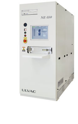
High-Density Plasma Etching System NE-550
NE550H is a multipurpose high-density plasma etching system, specifically for R&D test facilities such as universities and government agencies.
- Equipped with low-pressure, low-electron-temperature and high-density plasma source.
- Supports wide range of process control from ion etching to radical etching.
- Plasma density and uniformity can be controlled by optimizing magnetic field.
- Simple configuration makes maintenance easy.
- Low pressure, High density plasma, Good uniformity – ISM (Inductively Super Magnetron) Plasma Source* ULVAC Patent
- Good repeatability and stability – STAR Electrode* ULVAC Patent
- Precise and stable EPD – Optical Emission EPD (Optional), Laser Interference EPD (Optional)
- Precise wafer temperature control – ESC with He cooling, Mechanical Chuck
- Easy maintenance – Simple maintenance mechanism
Special Features / Further Applications
Films – Electronic Devices (HEMT, HBT, MMIC, etc..)
-
III-V materials: Selective etching – GaAs, AlGaAs, InGaAs, InGaP, InP
-
Insulating Layers: High speed or damage-free etching – SiO2, SiN, Low-K materials, GaAs VIA, InP VIA, SiC VIA
-
Organics: Polyimide, BCB
-
Metals and Ceramics: W, WSi, TiW, Mo, PZT, STO, BST, SBT, Ir, IrO2, Au, Pt, Ti, TiN, Ta Optical Devices (Laser Diodes, LED, etc..)
-
Non-selective etching – GaAs, AlGaAs, AlGaInP, InAlAs, InP, GaN, AlGaN, InGaN, AlN
-
ITO, Sapphire Other Devices (MEMS, Stamper for DVD, etc…)
- Si, SiC, Glass, Quartz, Sapphire, C, Diamond-like Carbon, Al, Cr, Mo
Further Applications
- Ultra-high frequency devices, optical devices (LEDs, LDs).
- Next-generation non-volatile memory.
- Bio-chips and micro-fluid devices.
- Photonic crystals.
- Sensors, MEMS (micro-electromechanical systems).


